


Bengaluru: CENS Display: A new easier technique of manufacturing liquid crystal displays-LCD has been developed CENS, which can reduce the cost of the devices. A team of scientists from the Centre for Nano and Soft Matter Sciences (CeNS), Bengaluru, an autonomous institute of the Department of Science and Technology (DST) conceptualized and implemented a novel way of employing a 2D materials to overcome the drawbacks of current methods.
An essential requirement of liquid crystal devices (LCDs- cens display) is the unidirectional planar alignment of the constituent liquid crystals (LC) over large areas.

Although the conventional polymer rubbing method yields quality LC alignment, it possesses unavoidable and undesirable drawbacks such as production of electrostatic charges and dust particles that interfere with display operation, and even cause damage to the electronic components of the display. While electrostatic charges increase the failure rate, dust creates defects which seriously compromises with the performance of the device. Other problems include multistep process for coating and the necessity for high-temperature curing. This has led to a surge in demand to replace this rubbing method with new non-contact techniques.
The latest among these techniques is to employ 2D nanomaterials – graphene, hexagonal boron nitride (h-BN), transition metal dichalcogenides, and so on as alignment layers. However, all these have a built-in lacuna owing to the deployment of the chemical vapour deposition (CVD) method as this technique necessitates high deposition temperature, necessity for precursors and by-products that are often hazardous or toxic. Besides, when the CVD method is used, unidirectional LC alignment is observed over only small regions.

Using h-BN nanoflakes as the specific material, the group comprising of Gayathri Pisharody, Priyabrata Sahoo, Dr. D.S. Shankar Rao, Dr. HSSR Matte and Dr. S. Krishna Prasad employed a procedure called solution-processed deposition technique and found it to be effective in getting the LC alignment over a much larger area. They also found the resultant crystals to be quite robust with no evidence of decay in LC orientation over several months.
The work published in ‘Advanced Materials Interfaces’ formed the basis for an Indian patent application. Lead researcher Dr. Prasad added that the method demonstrating a non-conventional and contact-free route for getting unidirectional alignment of LC, is also much simpler, scalable, flexible for adaptation, and cost-effective.
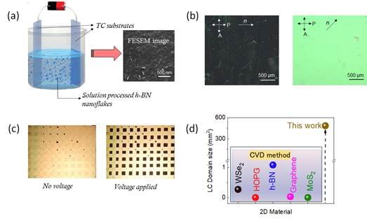
Figure 1: (a) Schematic showing the electrophoretic deposition (EPD) of h-BN nanoflakes over transparent conducting (TC) substrates and the FESEM image of the substrate, (b) The obtained birefringence when the polarizer is parallel and perpendicular/at 45o to the LC orientation, (c) Twisted Nematic (TN) configured LC device in the voltage ON and voltage OFF states showing high contrast ratio, and (d) Comparison of the alignment area obtained using CVD technique with the present research work.
Read Also | Coal Block Auction of Coal Mines for Commercial Mining
[amazon_auto_links id=”635″]